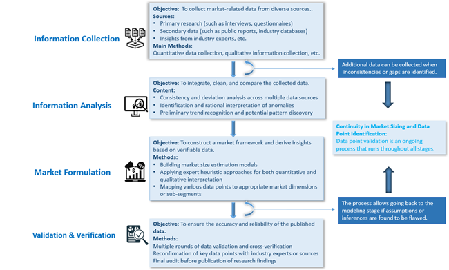
Definition and Scope: Semiconductor wafer inspection systems are advanced tools used in the semiconductor manufacturing process to detect defects on wafers at various stages of production. These systems employ sophisticated imaging techniques, such as optical inspection and electron microscopy, to identify imperfections like particles, scratches, or pattern deviations that could impact the functionality and performance of the final semiconductor devices. By providing real-time feedback on wafer quality, these inspection systems play a crucial role in ensuring high yields and overall product quality in the semiconductor industry. The market for semiconductor wafer inspection systems is experiencing significant growth driven by several key factors. Firstly, the increasing demand for smaller, more powerful semiconductors used in various electronic devices such as smartphones, laptops, and IoT devices is driving the need for higher precision and quality control in wafer manufacturing. Additionally, the rising complexity of semiconductor designs and processes necessitates more advanced inspection technologies to detect and address defects effectively. Moreover, the shift towards advanced packaging technologies like 3D ICs and heterogeneous integration further underscores the importance of reliable wafer inspection systems to maintain product integrity and performance. These market drivers are pushing semiconductor manufacturers to invest in state-of-the-art inspection solutions to meet the evolving demands of the industry. In addition to technological advancements and industry trends, the market for semiconductor wafer inspection systems is also influenced by factors such as increasing investments in R&D activities, the growing adoption of automation in semiconductor manufacturing, and the expanding semiconductor industry in regions like Asia Pacific. These developments are expected to drive further innovation in wafer inspection technologies, leading to more efficient, accurate, and high-throughput inspection systems that cater to the evolving needs of semiconductor manufacturers worldwide. The global Semiconductor Wafer Inspection System market size was estimated at USD 613.74 million in 2024, exhibiting a CAGR of 6.00% during the forecast period. This report offers a comprehensive analysis of the global Semiconductor Wafer Inspection System market, examining all key dimensions. It provides both a macro-level overview and micro-level market details, including market size, trends, competitive landscape, niche segments, growth drivers, and key challenges. Report Framework and Key Highlights: Market Dynamics: Identification of major market drivers, restraints, opportunities, and challenges. Trend Analysis: Examination of ongoing and emerging trends impacting the market. Competitive Landscape: Detailed profiles and market positioning of major players, including market share, operational status, product offerings, and strategic developments. Strategic Analysis Tools: SWOT Analysis, Porter’s Five Forces Analysis, PEST Analysis, Value Chain Analysis Market Segmentation: By type, application, region, and end-user industry. Forecasting and Growth Projections: In-depth revenue forecasts and CAGR analysis through 2033. This report equips readers with critical insights to navigate competitive dynamics and develop effective strategies. Whether assessing a new market entry or refining existing strategies, the report serves as a valuable tool for: Industry players Investors Researchers Consultants Business strategists And all stakeholders with an interest or investment in the Semiconductor Wafer Inspection System market. Global Semiconductor Wafer Inspection System Market: Segmentation Analysis and Strategic Insights This section of the report provides an in-depth segmentation analysis of the global Semiconductor Wafer Inspection System market. The market is segmented based on region (country), manufacturer, product type, and application. Segmentation enables a more precise understanding of market dynamics and facilitates targeted strategies across product development, marketing, and sales. By breaking the market into meaningful subsets, stakeholders can better tailor their offerings to the specific needs of each segment—enhancing competitiveness and improving return on investment. Global Semiconductor Wafer Inspection System Market: Market Segmentation Analysis The research report includes specific segments by region (country), manufacturers, Type, and Application. Market segmentation creates subsets of a market based on product type, end-user or application, Geographic, and other factors. By understanding the market segments, the decision-maker can leverage this targeting in the product, sales, and marketing strategies. Market segments can power your product development cycles by informing how you create product offerings for different segments. Key Companies Profiled KLA Corporation Applied Materials NanoRepro Hermes Microvision Hitachi High-Tech Group Tokyo Electron Device TSI TASMIT Inc Candella Instruments Vistec Semiconductor Systems Keysight ATM Group Cognex Corporation Hanmi Semiconductor MTI Instruments Shanghai RSIC Scientific Instrument Shenzhen Skyverse Technology MegaRobo Technologies Shenzhen Geling Jingrui Vision Dongguan Ruizhi Photoelectric Technology Teledyne DALSA Nikon Precision Newport Corporation Nidec Market Segmentation by Type EFEM Inspection System AOI Inspection System Market Segmentation by Application Foundries Memory Manufacturers Integrated Device Manufacturer(IDMs) Geographic Segmentation North America: United States, Canada, Mexico Europe: Germany, France, Italy, U.K., Spain, Sweden, Denmark, Netherlands, Switzerland, Belgium, Russia. Asia-Pacific: China, Japan, South Korea, India, Australia, Indonesia, Malaysia, Philippines, Singapore, Thailand South America: Brazil, Argentina, Colombia. Middle East and Africa (MEA): Saudi Arabia, United Arab Emirates, Egypt, Nigeria, South Africa, Rest of MEA Report Framework and Chapter Summary Chapter 1: Report Scope and Market Definition This chapter outlines the statistical boundaries and scope of the report. It defines the segmentation standards used throughout the study, including criteria for dividing the market by region, product type, application, and other relevant dimensions. It establishes the foundational definitions and classifications that guide the rest of the analysis. Chapter 2: Executive Summary This chapter presents a concise summary of the market’s current status and future outlook across different segments—by geography, product type, and application. It includes key metrics such as market size, growth trends, and development potential for each segment. The chapter offers a high-level overview of the Semiconductor Wafer Inspection System Market, highlighting its evolution over the short, medium, and long term. Chapter 3: Market Dynamics and Policy Environment This chapter explores the latest developments in the market, identifying key growth drivers, restraints, challenges, and risks faced by industry participants. It also includes an analysis of the policy and regulatory landscape affecting the market, providing insight into how external factors may shape future performance. Chapter 4: Competitive Landscape This chapter provides a detailed assessment of the market's competitive environment. It covers market share, production capacity, output, pricing trends, and strategic developments such as mergers, acquisitions, and expansion plans of leading players. This analysis offers a comprehensive view of the positioning and performance of top competitors. Chapters 5–10: Regional Market Analysis These chapters offer in-depth, quantitative evaluations of market size and growth potential across major regions and countries. Each chapter assesses regional consumption patterns, market dynamics, development prospects, and available capacity. The analysis helps readers understand geographical differences and opportunities in global markets. Chapter 11: Market Segmentation by Product Type This chapter examines the market based on product type, analyzing the size, growth trends, and potential of each segment. It helps stakeholders identify underexplored or high-potential product categories—often referred to as “blue ocean” opportunities. Chapter 12: Market Segmentation by Application This chapter analyzes the market based on application fields, providing insights into the scale and future development of each application segment. It supports readers in identifying high-growth areas across downstream markets. Chapter 13: Company Profiles This chapter presents comprehensive profiles of leading companies operating in the market. For each company, it details sales revenue, volume, pricing, gross profit margin, market share, product offerings, and recent strategic developments. This section offers valuable insight into corporate performance and strategy. Chapter 14: Industry Chain and Value Chain Analysis This chapter explores the full industry chain, from upstream raw material suppliers to downstream application sectors. It includes a value chain analysis that highlights the interconnections and dependencies across various parts of the ecosystem. Chapter 15: Key Findings and Conclusions The final chapter summarizes the main takeaways from the report, presenting the core conclusions, strategic recommendations, and implications for stakeholders. It encapsulates the insights drawn from all previous chapters. Table of Contents 1 Introduction to Research & Analysis Reports 1.1 Semiconductor Wafer Inspection System Market Definition 1.2 Semiconductor Wafer Inspection System Market Segments 1.2.1 Segment by Type 1.2.2 Segment by Application 2 Executive Summary 2.1 Global Semiconductor Wafer Inspection System Market Size 2.2 Market Segmentation – by Type 2.3 Market Segmentation – by Application 2.4 Market Segmentation – by Geography 3 Key Market Trends, Opportunity, Drivers and Restraints 3.1 Key Takeway 3.2 Market Opportunities & Trends 3.3 Market Drivers 3.4 Market Restraints 3.5 Market Major Factor Assessment 4 Global Semiconductor Wafer Inspection System Market Competitive Landscape 4.1 Global Semiconductor Wafer Inspection System Sales by Manufacturers (2020-2025) 4.2 Global Semiconductor Wafer Inspection System Revenue Market Share by Manufacturers (2020-2025) 4.3 Semiconductor Wafer Inspection System Market Share by Company Type (Tier 1, Tier 2, and Tier 3) 4.4 New Entrant and Capacity Expansion Plans 4.5 Mergers & Acquisitions 5 Global Semiconductor Wafer Inspection System Market by Region 5.1 Global Semiconductor Wafer Inspection System Market Size by Region 5.1.1 Global Semiconductor Wafer Inspection System Market Size by Region 5.1.2 Global Semiconductor Wafer Inspection System Market Size Market Share by Region 5.2 Global Semiconductor Wafer Inspection System Sales by Region 5.2.1 Global Semiconductor Wafer Inspection System Sales by Region 5.2.2 Global Semiconductor Wafer Inspection System Sales Market Share by Region 6 North America Market Overview 6.1 North America Semiconductor Wafer Inspection System Market Size by Country 6.1.1 USA Market Overview 6.1.2 Canada Market Overview 6.1.3 Mexico Market Overview 6.2 North America Semiconductor Wafer Inspection System Market Size by Type 6.3 North America Semiconductor Wafer Inspection System Market Size by Application 6.4 Top Players in North America Semiconductor Wafer Inspection System Market 7 Europe Market Overview 7.1 Europe Semiconductor Wafer Inspection System Market Size by Country 7.1.1 Germany Market Overview 7.1.2 France Market Overview 7.1.3 U.K. Market Overview 7.1.4 Italy Market Overview 7.1.5 Spain Market Overview 7.1.6 Sweden Market Overview 7.1.7 Denmark Market Overview 7.1.8 Netherlands Market Overview 7.1.9 Switzerland Market Overview 7.1.10 Belgium Market Overview 7.1.11 Russia Market Overview 7.2 Europe Semiconductor Wafer Inspection System Market Size by Type 7.3 Europe Semiconductor Wafer Inspection System Market Size by Application 7.4 Top Players in Europe Semiconductor Wafer Inspection System Market 8 Asia-Pacific Market Overview 8.1 Asia-Pacific Semiconductor Wafer Inspection System Market Size by Country 8.1.1 China Market Overview 8.1.2 Japan Market Overview 8.1.3 South Korea Market Overview 8.1.4 India Market Overview 8.1.5 Australia Market Overview 8.1.6 Indonesia Market Overview 8.1.7 Malaysia Market Overview 8.1.8 Philippines Market Overview 8.1.9 Singapore Market Overview 8.1.10 Thailand Market Overview 8.1.11 Rest of APAC Market Overview 8.2 Asia-Pacific Semiconductor Wafer Inspection System Market Size by Type 8.3 Asia-Pacific Semiconductor Wafer Inspection System Market Size by Application 8.4 Top Players in Asia-Pacific Semiconductor Wafer Inspection System Market 9 South America Market Overview 9.1 South America Semiconductor Wafer Inspection System Market Size by Country 9.1.1 Brazil Market Overview 9.1.2 Argentina Market Overview 9.1.3 Columbia Market Overview 9.2 South America Semiconductor Wafer Inspection System Market Size by Type 9.3 South America Semiconductor Wafer Inspection System Market Size by Application 9.4 Top Players in South America Semiconductor Wafer Inspection System Market 10 Middle East and Africa Market Overview 10.1 Middle East and Africa Semiconductor Wafer Inspection System Market Size by Country 10.1.1 Saudi Arabia Market Overview 10.1.2 UAE Market Overview 10.1.3 Egypt Market Overview 10.1.4 Nigeria Market Overview 10.1.5 South Africa Market Overview 10.2 Middle East and Africa Semiconductor Wafer Inspection System Market Size by Type 10.3 Middle East and Africa Semiconductor Wafer Inspection System Market Size by Application 10.4 Top Players in Middle East and Africa Semiconductor Wafer Inspection System Market 11 Semiconductor Wafer Inspection System Market Segmentation by Type 11.1 Evaluation Matrix of Segment Market Development Potential (Type) 11.2 Global Semiconductor Wafer Inspection System Sales Market Share by Type (2020-2033) 11.3 Global Semiconductor Wafer Inspection System Market Size Market Share by Type (2020-2033) 11.4 Global Semiconductor Wafer Inspection System Price by Type (2020-2033) 12 Semiconductor Wafer Inspection System Market Segmentation by Application 12.1 Evaluation Matrix of Segment Market Development Potential (Application) 12.2 Global Semiconductor Wafer Inspection System Market Sales by Application (2020-2033) 12.3 Global Semiconductor Wafer Inspection System Market Size (M USD) by Application (2020-2033) 12.4 Global Semiconductor Wafer Inspection System Sales Growth Rate by Application (2020-2033) 13 Company Profiles 13.1 KLA Corporation 13.1.1 KLA Corporation Company Overview 13.1.2 KLA Corporation Business Overview 13.1.3 KLA Corporation Semiconductor Wafer Inspection System Major Product Offerings 13.1.4 KLA Corporation Semiconductor Wafer Inspection System Sales and Revenue fromSemiconductor Wafer Inspection System (2020-2025) 13.1.5 Key News 13.2 Applied Materials 13.2.1 Applied Materials Company Overview 13.2.2 Applied Materials Business Overview 13.2.3 Applied Materials Semiconductor Wafer Inspection System Major Product Offerings 13.2.4 Applied Materials Semiconductor Wafer Inspection System Sales and Revenue fromSemiconductor Wafer Inspection System (2020-2025) 13.2.5 Key News 13.3 NanoRepro 13.3.1 NanoRepro Company Overview 13.3.2 NanoRepro Business Overview 13.3.3 NanoRepro Semiconductor Wafer Inspection System Major Product Offerings 13.3.4 NanoRepro Semiconductor Wafer Inspection System Sales and Revenue fromSemiconductor Wafer Inspection System (2020-2025) 13.3.5 Key News 13.4 Hermes Microvision 13.4.1 Hermes Microvision Company Overview 13.4.2 Hermes Microvision Business Overview 13.4.3 Hermes Microvision Semiconductor Wafer Inspection System Major Product Offerings 13.4.4 Hermes Microvision Semiconductor Wafer Inspection System Sales and Revenue fromSemiconductor Wafer Inspection System (2020-2025) 13.4.5 Key News 13.5 Hitachi High-Tech Group 13.5.1 Hitachi High-Tech Group Company Overview 13.5.2 Hitachi High-Tech Group Business Overview 13.5.3 Hitachi High-Tech Group Semiconductor Wafer Inspection System Major Product Offerings 13.5.4 Hitachi High-Tech Group Semiconductor Wafer Inspection System Sales and Revenue fromSemiconductor Wafer Inspection System (2020-2025) 13.5.5 Key News 13.6 Tokyo Electron Device 13.6.1 Tokyo Electron Device Company Overview 13.6.2 Tokyo Electron Device Business Overview 13.6.3 Tokyo Electron Device Semiconductor Wafer Inspection System Major Product Offerings 13.6.4 Tokyo Electron Device Semiconductor Wafer Inspection System Sales and Revenue fromSemiconductor Wafer Inspection System (2020-2025) 13.6.5 Key News 13.7 TSI 13.7.1 TSI Company Overview 13.7.2 TSI Business Overview 13.7.3 TSI Semiconductor Wafer Inspection System Major Product Offerings 13.7.4 TSI Semiconductor Wafer Inspection System Sales and Revenue fromSemiconductor Wafer Inspection System (2020-2025) 13.7.5 Key News 13.8 TASMIT 13.8.1 TASMIT Company Overview 13.8.2 TASMIT Business Overview 13.8.3 TASMIT Semiconductor Wafer Inspection System Major Product Offerings 13.8.4 TASMIT Semiconductor Wafer Inspection System Sales and Revenue fromSemiconductor Wafer Inspection System (2020-2025) 13.8.5 Key News 13.9 Inc 13.9.1 Inc Company Overview 13.9.2 Inc Business Overview 13.9.3 Inc Semiconductor Wafer Inspection System Major Product Offerings 13.9.4 Inc Semiconductor Wafer Inspection System Sales and Revenue fromSemiconductor Wafer Inspection System (2020-2025) 13.9.5 Key News 13.10 Candella Instruments 13.10.1 Candella Instruments Company Overview 13.10.2 Candella Instruments Business Overview 13.10.3 Candella Instruments Semiconductor Wafer Inspection System Major Product Offerings 13.10.4 Candella Instruments Semiconductor Wafer Inspection System Sales and Revenue fromSemiconductor Wafer Inspection System (2020-2025) 13.10.5 Key News 13.11 Vistec Semiconductor Systems 13.11.1 Vistec Semiconductor Systems Company Overview 13.11.2 Vistec Semiconductor Systems Business Overview 13.11.3 Vistec Semiconductor Systems Semiconductor Wafer Inspection System Major Product Offerings 13.11.4 Vistec Semiconductor Systems Semiconductor Wafer Inspection System Sales and Revenue fromSemiconductor Wafer Inspection System (2020-2025) 13.11.5 Key News 13.12 Keysight 13.12.1 Keysight Company Overview 13.12.2 Keysight Business Overview 13.12.3 Keysight Semiconductor Wafer Inspection System Major Product Offerings 13.12.4 Keysight Semiconductor Wafer Inspection System Sales and Revenue fromSemiconductor Wafer Inspection System (2020-2025) 13.12.5 Key News 13.13 ATM Group 13.13.1 ATM Group Company Overview 13.13.2 ATM Group Business Overview 13.13.3 ATM Group Semiconductor Wafer Inspection System Major Product Offerings 13.13.4 ATM Group Semiconductor Wafer Inspection System Sales and Revenue fromSemiconductor Wafer Inspection System (2020-2025) 13.13.5 Key News 13.14 Cognex Corporation 13.14.1 Cognex Corporation Company Overview 13.14.2 Cognex Corporation Business Overview 13.14.3 Cognex Corporation Semiconductor Wafer Inspection System Major Product Offerings 13.14.4 Cognex Corporation Semiconductor Wafer Inspection System Sales and Revenue fromSemiconductor Wafer Inspection System (2020-2025) 13.14.5 Key News 13.15 Hanmi Semiconductor 13.15.1 Hanmi Semiconductor Company Overview 13.15.2 Hanmi Semiconductor Business Overview 13.15.3 Hanmi Semiconductor Semiconductor Wafer Inspection System Major Product Offerings 13.15.4 Hanmi Semiconductor Semiconductor Wafer Inspection System Sales and Revenue fromSemiconductor Wafer Inspection System (2020-2025) 13.15.5 Key News 13.16 MTI Instruments 13.16.1 MTI Instruments Company Overview 13.16.2 MTI Instruments Business Overview 13.16.3 MTI Instruments Semiconductor Wafer Inspection System Major Product Offerings 13.16.4 MTI Instruments Semiconductor Wafer Inspection System Sales and Revenue fromSemiconductor Wafer Inspection System (2020-2025) 13.16.5 Key News 13.17 Shanghai RSIC Scientific Instrument 13.17.1 Shanghai RSIC Scientific Instrument Company Overview 13.17.2 Shanghai RSIC Scientific Instrument Business Overview 13.17.3 Shanghai RSIC Scientific Instrument Semiconductor Wafer Inspection System Major Product Offerings 13.17.4 Shanghai RSIC Scientific Instrument Semiconductor Wafer Inspection System Sales and Revenue fromSemiconductor Wafer Inspection System (2020-2025) 13.17.5 Key News 13.18 Shenzhen Skyverse Technology 13.18.1 Shenzhen Skyverse Technology Company Overview 13.18.2 Shenzhen Skyverse Technology Business Overview 13.18.3 Shenzhen Skyverse Technology Semiconductor Wafer Inspection System Major Product Offerings 13.18.4 Shenzhen Skyverse Technology Semiconductor Wafer Inspection System Sales and Revenue fromSemiconductor Wafer Inspection System (2020-2025) 13.18.5 Key News 13.19 MegaRobo Technologies 13.19.1 MegaRobo Technologies Company Overview 13.19.2 MegaRobo Technologies Business Overview 13.19.3 MegaRobo Technologies Semiconductor Wafer Inspection System Major Product Offerings 13.19.4 MegaRobo Technologies Semiconductor Wafer Inspection System Sales and Revenue fromSemiconductor Wafer Inspection System (2020-2025) 13.19.5 Key News 13.20 Shenzhen Geling Jingrui Vision 13.20.1 Shenzhen Geling Jingrui Vision Company Overview 13.20.2 Shenzhen Geling Jingrui Vision Business Overview 13.20.3 Shenzhen Geling Jingrui Vision Semiconductor Wafer Inspection System Major Product Offerings 13.20.4 Shenzhen Geling Jingrui Vision Semiconductor Wafer Inspection System Sales and Revenue fromSemiconductor Wafer Inspection System (2020-2025) 13.20.5 Key News 13.21 Dongguan Ruizhi Photoelectric Technology 13.21.1 Dongguan Ruizhi Photoelectric Technology Company Overview 13.21.2 Dongguan Ruizhi Photoelectric Technology Business Overview 13.21.3 Dongguan Ruizhi Photoelectric Technology Semiconductor Wafer Inspection System Major Product Offerings 13.21.4 Dongguan Ruizhi Photoelectric Technology Semiconductor Wafer Inspection System Sales and Revenue fromSemiconductor Wafer Inspection System (2020-2025) 13.21.5 Key News 13.22 Teledyne DALSA 13.22.1 Teledyne DALSA Company Overview 13.22.2 Teledyne DALSA Business Overview 13.22.3 Teledyne DALSA Semiconductor Wafer Inspection System Major Product Offerings 13.22.4 Teledyne DALSA Semiconductor Wafer Inspection System Sales and Revenue fromSemiconductor Wafer Inspection System (2020-2025) 13.22.5 Key News 13.23 Nikon Precision 13.23.1 Nikon Precision Company Overview 13.23.2 Nikon Precision Business Overview 13.23.3 Nikon Precision Semiconductor Wafer Inspection System Major Product Offerings 13.23.4 Nikon Precision Semiconductor Wafer Inspection System Sales and Revenue fromSemiconductor Wafer Inspection System (2020-2025) 13.23.5 Key News 13.24 Newport Corporation 13.24.1 Newport Corporation Company Overview 13.24.2 Newport Corporation Business Overview 13.24.3 Newport Corporation Semiconductor Wafer Inspection System Major Product Offerings 13.24.4 Newport Corporation Semiconductor Wafer Inspection System Sales and Revenue fromSemiconductor Wafer Inspection System (2020-2025) 13.24.5 Key News 13.25 Nidec 13.25.1 Nidec Company Overview 13.25.2 Nidec Business Overview 13.25.3 Nidec Semiconductor Wafer Inspection System Major Product Offerings 13.25.4 Nidec Semiconductor Wafer Inspection System Sales and Revenue fromSemiconductor Wafer Inspection System (2020-2025) 13.25.5 Key News 13.25.6 Key News 14 Key Market Trends, Opportunity, Drivers and Restraints 14.1 Key Takeway 14.2 Market Opportunities & Trends 14.3 Market Drivers 14.4 Market Restraints 14.5 Market Major Factor Assessment 14.6 Porter's Five Forces Analysis of Semiconductor Wafer Inspection System Market 14.7 PEST Analysis of Semiconductor Wafer Inspection System Market 15 Analysis of the Semiconductor Wafer Inspection System Industry Chain 15.1 Overview of the Industry Chain 15.2 Upstream Segment Analysis 15.3 Midstream Segment Analysis 15.3.1 Manufacturing, Processing or Conversion Process Analysis 15.3.2 Key Technology Analysis 15.4 Downstream Segment Analysis 15.4.1 Downstream Customer List and Contact Details 15.4.2 Customer Concerns or Preference Analysis 16 Conclusion 17 Appendix 17.1 Methodology 17.2 Research Process and Data Source 17.3 Disclaimer 17.4 Note 17.5 Examples of Clients 17.6 DisclaimerResearch Methodology The research methodology employed in this study follows a structured, four-stage process designed to ensure the accuracy, consistency, and relevance of all data and insights presented. The process begins with Information Procurement, wherein data is collected from a wide range of primary and secondary sources. This is followed by Information Analysis, during which the collected data is systematically mapped, discrepancies across sources are examined, and consistency is established through cross-validation.
Subsequently, the Market Formulation phase involves placing verified data points into an appropriate market context to generate meaningful conclusions. This step integrates analyst interpretation and expert heuristics to refine findings and ensure applicability. Finally, all conclusions undergo a rigorous Validation and Publishing process, where each data point is re-evaluated before inclusion in the final deliverable. The methodology emphasizes bidirectional flow and reversibility between key stages to maintain flexibility and reinforce the integrity of the analysis.
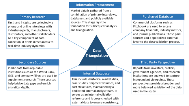
Research Process The market research process follows a structured and iterative methodology designed to ensure accuracy, depth, and reliability. It begins with scope definition and research design, where the research objectives are clearly outlined based on client requirements, emerging market trends, and initial exploratory insights. This phase provides strategic direction for all subsequent stages of the research. Data collection is then conducted through both secondary and primary research. Secondary research involves analyzing publicly available and paid sources such as company filings, industry journals, and government databases to build foundational knowledge. This is followed by primary research, which includes direct interviews and surveys with key industry stakeholders—such as manufacturers, distributors, and end users—to gather firsthand insights and address data gaps identified earlier. Techniques included CATI (Computer-Assisted Telephonic Interviewing), CAWI (Computer-Assisted Web Interviewing), CAVI (Computer-Assisted Video Interviewing via platforms like Zoom and WebEx), and CASI (Computer-Assisted Self Interviewing via email or LinkedIn).